What is a bipolar transistor and what is its feature
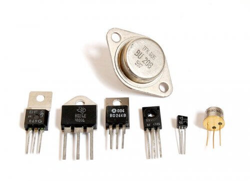
The word "transistor" is composed of the words TRANSfer and resISTOR - resistance converter. He replaced lamps in the early 1950s. This is a three-pin device used for amplification and switching in electronic circuits. The adjective “bipolar” (bipolar junction transistor) serves to distinguish from field effect transistors (FET). The principle of operation of a bipolar transistor is to use two p-n junctions forming a barrier layer, which allows a small current to controlaboutwith the highest current. The bipolar transistor is used both as a controlled resistance and as a key. Transistors are of two types: pnp and npn.
P-N junction
Germanium (Ge) and silicon (Si) are semiconductors. Now mainly silicon is used. The valency of Si and Ge is four. Therefore, if we add pentavalent arsenic to the crystal lattice of silicon (As), we get an “extra” electron, and if we add trivalent boron (B), we get a vacant place for an electron. In the first case, they speak of a “donor” material giving electrons, in the second case they speak of an “acceptor” material receiving electrons. Also, the first type of material is called N (negative), and the second - P (positive).
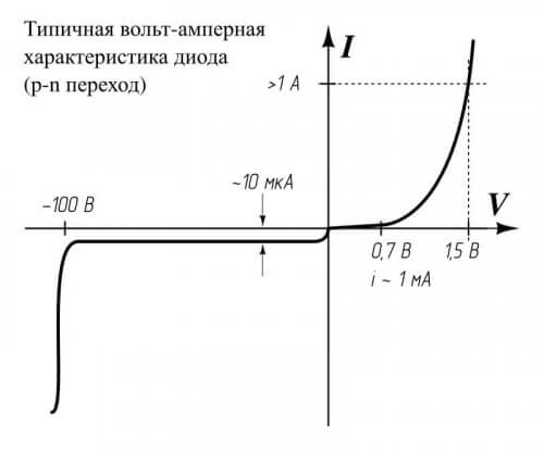
If materials of P and N types are brought into contact, a current will arise between them and a dynamic equilibrium will be established with a depleted region, where the concentration of charge carriers — electrons and vacant sites (“holes”) - is small. This layer has one-sided conductivity and serves as the basis for a device called a diode. Direct contact of materials will not create a qualitative transition; alloying (diffusion) or “clogging” of dopant ions into a crystal in a vacuum is necessary.
PNP transistor
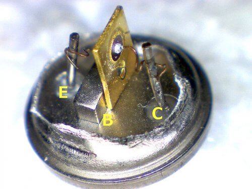
For the first time, a bipolar transistor was made by melting indium droplets into a germanium crystal (n-type material). Indium (In) is a trivalent metal, p-type material. Therefore, such a transistor was called diffuse (alloyed) having a p-n-p (or pnp) structure. The bipolar transistor in the figure below was manufactured in 1965. Its body is cut for clarity.
The germanium crystal in the center is called the base, and the indium droplets melted into it are called the emitter and collector. It is possible to consider transitions EB (emitter) and KB (collector) as ordinary diodes, but the transition CE (collector-emitter) has a special property. Therefore, it is impossible to manufacture a bipolar transistor from two separate diodes.
If a voltage of several volts is applied between the collector (-) and the emitter (+) in a pnp type transistor, a very weak current, a few μA, will flow in the circuit. If then a small (opening) voltage is applied between the base (-) and the emitter (+) - for germanium it is about 0.3 V (and for silicon 0.6 V) - then a current of some magnitude will flow from the emitter to the base.But since the base is made very thin, it will quickly become saturated with holes (it “loses” its excess of electrons that will go to the emitter). Since the emitter is heavily doped with hole conduction, and the recombination of electrons in the weakly doped base is a little delayed, thenaboutmost of the current will flow from the emitter to the collector. The collector is made larger than the emitter and slightly doped, which allows it to haveaboutlower breakdown voltage (USample CE> USample EB) Also, since the bulk of the holes recombine in the collector, it heats up more strongly than the other electrodes of the device.
Between the collector and emitter current there is a ratio:
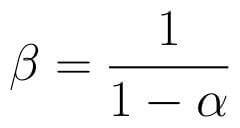
Typically, α lies in the range of 0.85-0.999 and inversely depends on the thickness of the base. This value is called the emitter current transfer coefficient. In practice, the reciprocal is often used (also denoted by h21e):
This is the base current transfer coefficient, one of the most important parameters of a bipolar transistor. It more often determines the enhancing properties in practice.
The PNP transistor is called the forward conductor transistor. But there is another type of transistor, the structure of which perfectly complements pnp in circuitry.
NPN transistor
The bipolar transistor may have a collector with an emitter of N-type material. Then the base is made of P-type material. And in this case, the npn transistor works exactly like pnp, with the exception of polarity - it is a reverse conductivity transistor.
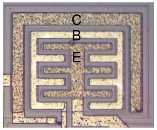
Silicon-based transistors suppress with their numbers all other types of bipolar transistors. As a donor material for the collector and emitter can serve as As, having an "extra" electron. The technology for manufacturing transistors has also changed. Now they are planar, which makes it possible to use lithography and make integrated circuits. The picture below shows a planar bipolar transistor (as part of an integrated circuit at high magnification). According to planar technology, both pnp and npn transistors are manufactured, including powerful ones. Alloy are already discontinued.
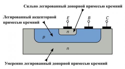
The planar bipolar transistor in the context of the following picture (simplified diagram).
The picture shows how well the design of the planar transistor is arranged - the collector is effectively cooled by the crystal substrate. A planar pnp transistor is also manufactured.
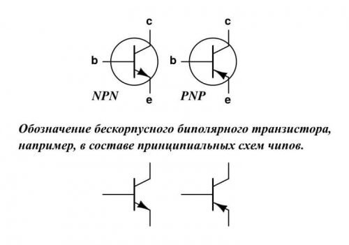
Conventional graphic designations of a bipolar transistor are shown in the following picture.
These UGOs are international, and also valid in accordance with GOST 2.730-73.
Transistor Switching Circuits
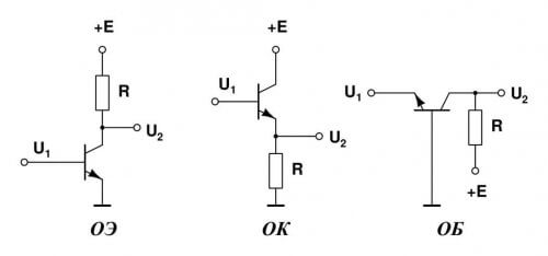
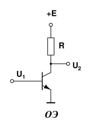
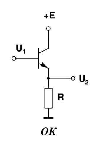
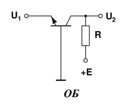
Usually a bipolar transistor is always used in direct connection - the reverse polarity at the FE junction gives nothing interesting. For a direct connection scheme, there are three connection schemes: a common emitter (OE), a common collector (OK), and a common base (OB). All three inclusions are shown below. They explain only the principle of operation itself - assuming that the operating point is somehow installed using an additional power source or auxiliary circuit. To open a silicon transistor (Si), it is necessary to have a potential of ~ 0.6 V between the emitter and the base, and for a germanium it is enough ~ 0.3 V.
Common emitter
The voltage U1 causes a current Ib, the collector current Ik is equal to the base current multiplied by β. In this case, the voltage + E should be large enough: 5 V-15 V. This circuit amplifies the current and voltage well, and therefore, the power. The output signal is opposite in phase to the input (inverted). This is used in digital technology as a function of NOT.
If the transistor does not work in the key mode, but as an amplifier of small signals (active or linear mode), then, using the selection of the base current, the voltage U is set2 equal to E / 2 so that the output signal is not distorted. Such an application is used, for example, in amplifying audio signals in high-end amplifiers with low distortion and, as a result, low efficiency.
Common collector
In terms of voltage, the OK circuit does not amplify, here the gain is α ~ 1.Therefore, this circuit is called an emitter follower. The current in the emitter circuit is β + 1 times greater than in the base circuit. This circuit amplifies the current well and has a low output and very high input impedance. (This is the time to remember that the transistor is called a resistance transformer.)
The emitter follower has properties and operating parameters that are very suitable for oscilloscope probes. It uses its huge input impedance and low output, which is good for matching with a low-impedance cable.
Common base
This circuit is characterized by the lowest input resistance, but its current gain is equal to α. A common base circuit amplifies well in voltage, but not in power. Its feature is the elimination of the influence of feedback on capacitance (eff. Miller). Cascades with OBs are ideally suited as input stages of amplifiers in radio frequency paths matched at low resistances of 50 and 75 Ohms.
Cascades with a common base are very widely used in microwave technology and their use in radio electronics with a cascade of emitter followers is very common.
Two main operating modes
Distinguish between modes of operation using the "small" and "large" signal. In the first case, the bipolar transistor operates in a small area of its characteristics and this is used in analog technology. In such cases, the linearity of signal amplification and low noise are important. This is a linear mode.
In the second case (key mode), the bipolar transistor operates in the full range - from saturation to cut-off, like a key. This means that if you look at the I – V characteristics of the pn junction, you should apply a small reverse voltage between the base and emitter to completely lock the transistor, and to fully open when the transistor goes into saturation mode, slightly increase the base current compared to the low-signal mode. Then the transistor works like a pulse switch. This mode is used in switching and power devices, it is used for switching power supplies. In such cases, they try to achieve a short switching time of the transistors.
Digital logic is characterized by an intermediate position between the “large” and “small” signals. A low logic level is limited by 10% of the supply voltage, and a high one by 90%. Time delays and switching seek to reduce to the limit. This mode of operation is key, but they seek to minimize power here. Any logical element is a key.
Other types of transistors
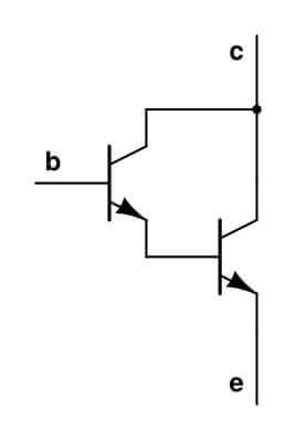
The main types of transistors already described do not limit their arrangement. Composite transistors are produced (Darlington circuit). Their β is very large and equal to the product of the coefficients of both transistors, therefore they are also called “superbet" transistors.
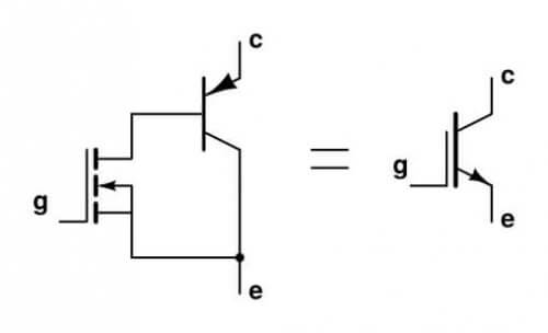
Electrical engineering has already mastered IGBTs (insulated gate bipolar transistor), with an isolated gate. The gate of the field effect transistor is indeed isolated from its channel. True, there is a question of recharging its input capacitance during switching, so, without current, it can not do here.
Such transistors are used in powerful power switches: pulse converters, inverters, etc. The input IGBTs are very sensitive due to the high gate resistance of the field effect transistors. On exit - they give the opportunity to receive huge currents and can be manufactured for high voltage. For example, in the USA there is a new solar power station, where such transistors in the bridge circuit are loaded with powerful transformers that transfer energy to the industrial network.
In conclusion, we note that transistors, in simple words, are the “workhorse" of all modern electronics. They are used everywhere: from electric locomotives to mobile phones. Any modern computer consists of almost all transistors. The physical foundations of the operation of transistors are well understood and promise many more new achievements.
Related materials:

